
There’s nothing I love more than tearing down a console – seeing a popular electronic device dismantled to its core, revealing… well, usually something much simpler than you might expect. We’ve seen people tear down the PlayStation 5 Pro in the past, but last week, Sony finally revealed its own teardown, sharing a wealth of amazing details that give us a remarkable insight into how much engineering goes into creating a modern console.
From a personal perspective, the biggest surprise I had when I received my own PS5 Pro last November was how small it was. We had heard about leaked specifications, expected a very large processor with reduced graphic clock speeds compared to RDNA 3 and RDNA 4 graphics cards, expected a 6nm chip supported by a substantial cooling setup. The expectation was a unit with a volume similar to that of the original PlayStation 5, but we were wrong.
Sony’s Teardown Analysis
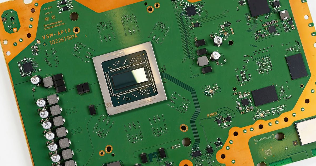
Sony’s analysis arrived in the same week that a PS5 Pro motherboard arrived at my house (yes, it’s weird, but I collect console motherboards, mainly for photographic purposes when it comes to video content). Upon opening the package, I was impressed by a board that is not much larger than the equivalent of the PS5 Slim. The relatively small increase in board size is accompanied by a surprisingly small difference in the size of the main processor. The chip of about 279 mm² of the new Pro is not much larger than the 260 mm² of the Slim, leading us to believe that Sony is using a more modern 4nm process technology, like that used in the latest consumer graphics cards.

Efficient Design of the PS5 Pro
Looking at that small board, one can see again how efficient the design is. When the PS5 Pro was announced, there seemed to be a rush of gamers and journalists wanting to build more powerful PCs for the same price. I haven’t seen any convincing proof that this was possible at the time and still don’t see it now, unless you want to add a few years of PlayStation Plus subscriptions. The CPU, GPU, and a series of other logic are contained in that single processor. Memory for all system functions is shared by eight main GDDR6 modules, with a ninth 2GB DDR5 added to handle slower system functions, leaving faster RAM for games. A new WiFi module was added, while the integrated SSD looks very similar to that of the PS5 Slim, just with dual-capacity modules.
The modular nature of a PC has many advantages – being able to choose specific components means you can create your own gaming machine built to your liking. This means you can take advantage of a competitive market to get deals on individual components. The PS5 and Pro motherboards demonstrate the advantages of a highly integrated design – the PC reduced to its essentials. And with that fixed architecture comes the surrounding industrial design, where Sony’s teardown reveals many new details.
The “blinds” of the Sony – the slats in the center of the unit – were designed to minimize the fan noise coming from the front of the unit. The surface area of the openings on the back, along with the size of the single internal fan, were increased compared to the basic PS5 to accommodate the 40 W increase in the main processor’s performance. Blades were added along the fan blades to increase cooling while maintaining silence – a stark contrast to the previous generation’s PS4 Pro. My favorite detail of the industrial design comes from the number of screws attached to the internal metal shielding. Notably, the quantity of screws and their placement reduce the amount of electromagnetic interference that could disrupt other electronic devices.
Similarities in cooling configuration exist with the existing PlayStation 5 in other aspects. A heatsink with a large surface area with copper tubes is nothing new, nor is the use of liquid metal as a thermal interface material. However, more copper tubes have been added to improve heat transfer, while the main contact point with the system processor now has a series of grooves. There have been reports that the standard PS5’s liquid metal becomes less uniform over time when the console is in the vertical position. These grooves should help keep the liquid metal TIM more evenly spread over the chip over the years.
In addition to the larger GPU and new features embedded in the silicon, there is a clear sense of continuity with the design of the PS5 Pro, whose lineage dates back to the original PS4: a single system-on-chip surrounded by memory modules that dominate the board, but built on the philosophy of custom PC technologies and consolidated into a sleek and economical design. Mark Cerny called it a super-powerful PC architecture when he introduced the PS4, and that philosophy remains to this day. So, what’s next? And based on the high retail price of the PS5 Pro, will it be affordable?
PlayStation 6 Hardware Expectations
At this point, we are expecting two pieces of hardware based on the PlayStation 6. There will be a standard console – naturally – and there are also plans for a portable console. According to the famous leaker KeplerL2, who provided accurate information about the PS5 Pro before its release, the chip for the mobile device will be manufactured on a 3nm manufacturing node. I would expect something similar for the PS6 as well – an interesting evolution of Microsoft’s Series X/S strategy – a unified architecture, with a more powerful processor for the home console. The 3nm process allegedly offers a 1.7x improvement in logic density compared to the technology used in the PS5 Pro, so depending on the cost of the chip and the innovations of AMD’s next-generation architectures, there is room for a complete generational leap. The question that remains is the cost – but with Microsoft and Sony committed to a tenth-generation console, we have to assume that the economics make sense, even if costs may continue to be a challenge for the end user.
Potential Console Design Evolution
Looking at the analysis of the PS5 Pro, I think the question is how far the console design can evolve beyond that basic design. The PS4 introduced us to the AMD APU surrounded by unified memory. The PS5 brought the storage from an external mechanical drive to an integrated solid-state solution, while Sony’s team placed more emphasis on a quieter design. In the world of PCs, AMD’s experiences with its remarkable Strix Halo processor show that the company is moving towards a chiplet-based design – the idea that smaller processors connected in the same package can offer cost reductions compared to a monolithic piece of silicon. It seems extraordinarily complex and expensive for a console, but who knows what comes next – and remember that we still have Microsoft’s claims about the tenth generation as “the biggest technological leap ever” in a hardware generation to consider. Machine learning will be crucial for this, but it’s still a difficult statement to reconcile – but perhaps the next-generation analyses will reveal everything.